

 Thought Leadership
IBM has unveiled what it describes as the world’s first 0.7-nanometer transistor technology, pushing semiconductor design into the sub-1nm regime. The new three-dimensional “Nanostack” architecture is said to nearly double transistor density compared to previous generations.
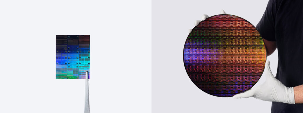
At its Yorktown Heights research facility, IBM introduced a next-generation semiconductor process operating at a scale of 0.7 nanometers, equivalent to 7 angstroms. The breakthrough enables nearly 100 billion transistors to be packed into an area the size of a fingernail.
Compared to IBM’s 2-nanometer chips announced in 2021, this represents close to a twofold increase in transistor density. The gain is made possible by a new transistor design called Nanostack. The architecture uses vertically stacked nanosheet-based transistors arranged in a staggered 3D layout, significantly improving silicon area efficiency.
Higher throughput and improved energy efficiency
The company says the new technology could deliver substantial performance gains for generative AI workloads and cloud infrastructure. Technical estimates suggest up to 50% higher computing performance or up to 70% lower energy consumption compared to 2-nanometer chips.
Research presented at VLSI 2026 also indicates that the Nanostack architecture enables a 40% scaling improvement in static RAM capacity. Jay Gambetta, Director of IBM Research, put the development into context:
“IBM’s latest chip breakthrough marks a milestone in computing, pushing technology beyond the nanometer era into the atomic scale. With our Nanostack architecture, we are not just shrinking transistors—we are reinventing how chips are built to deliver dramatically higher performance and energy efficiency.”
Jay Gambetta, Director of IBM Research
Industry collaboration and path to production
The development work was carried out at IBM’s semiconductor research center in Albany, New York. Future process development will leverage high-numerical-aperture extreme ultraviolet (EUV) lithography systems, designed to print more precise circuit patterns.
The EUV tools are being developed by ASML. IBM is also collaborating with partners including Lam Research, Tokyo Electron, and Screen Semiconductor Solutions to advance manufacturing technologies.
IBM expects the sub-1-nanometer Nanostack process to reach production readiness within the next five years. In parallel, the company plans to spin off a standalone entity called Anderon, which will operate as a dedicated quantum foundry supporting the production of quantum wafers.
(ll)